
If you have ever examined the internal architecture of a modern high-performance smartphone, a premium wearable device, or advanced audio equipment, you have likely been impressed by the density of integration within such a confined volume. Beneath the display and circuit boards lies an ecosystem of miniature metal components performing critical mechanical functions. These include micro-hinges enabling foldable displays to operate smoothly through thousands of cycles, high-density connectors transmitting substantial data streams through sub-miniature ports, and electromagnetic shielding frames ensuring signal integrity amid crowded spectra. The electronics sector is driven by an unrelenting mandate for miniaturization and performance enhancement, placing extreme demands on the metallic constituents within these assemblies.
For years, engineers have leveraged two primary technologies to fabricate these small-scale metallic features: Additive Manufacturing (AM) and Metal Injection Molding (MIM). On the surface, 3D printing appears ideally suited for generating complex internal lattices and organic topologies that conventional machining cannot replicate. However, when production forecasts escalate into the hundreds of thousands or millions of units, the layer-by-layer economics of laser-based powder bed fusion begin to diverge from commercial viability. This presents a critical decision point for engineering teams: at what threshold does it become advantageous to forgo the flexibility of the laser in favor of the repeatability of a MIM tool? The answer resides not strictly in geometric complexity, but in the physics of production volume, surface finish, and precision tolerance.
The Electronics Sector's Unique Requirements Beyond Miniaturization
It is a misconception that small size automatically dictates MIM, or that geometric complexity mandates AM. In consumer technology applications, the decision matrix is exceptionally stringent due to demanding tolerance bands and uncompromising aesthetic requirements. The component in question is not a hidden internal bracket; it may be a user-facing interface element that is handled daily, or a sealing mechanism requiring both tactile fluidity and environmental resistance.
Surface finish and tactile perception are therefore critical metrics. Laser Powder Bed Fusion (L-PBF) inherently produces a characteristic surface texture resulting from partially sintered powder adhesion. While acceptable for many mechanical applications, this texture can be a liability in electronics. It may trap particulate contaminants, detract from perceived product quality, or introduce undesirable friction in kinematic assemblies such as button stems or rotating crowns.
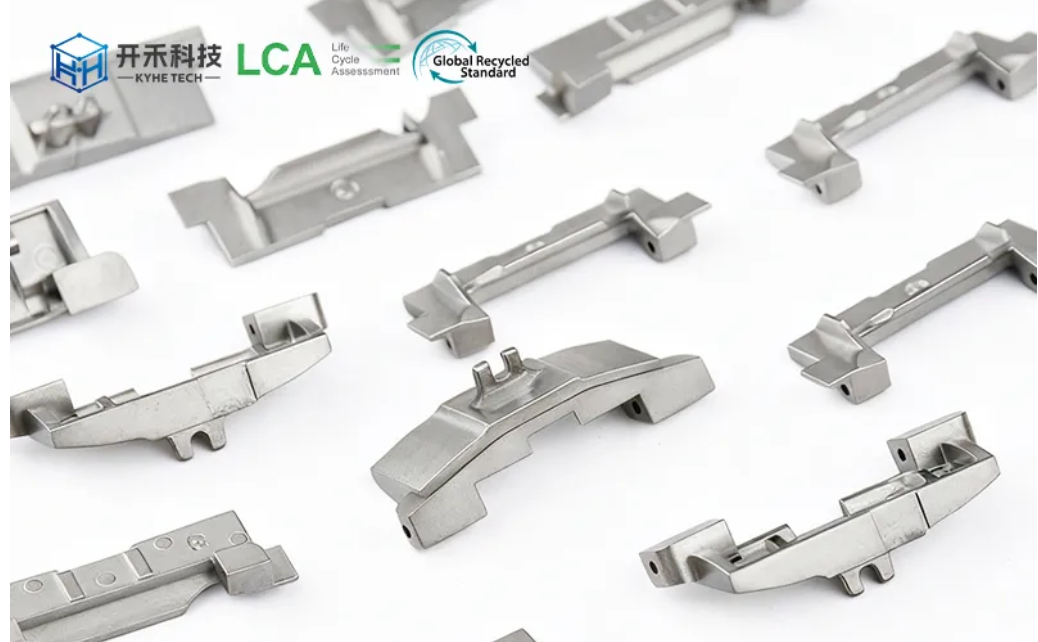
In contrast, components produced via Metal Injection Molding emerge from the sintering cycle with a surface roughness profile that is significantly closer to a refined, polished, or machined state. The resulting part feels dense and premium. This tactile distinction carries substantial weight in user experience design. Experienced production partners often guide clients toward MIM for high-volume electronics specifically because of this end-user perception factor. While AM parts can be post-processed to achieve a similar finish, each additional step introduces cost and variability into a workflow that MIM accomplishes intrinsically at scale. Once production volumes exceed approximately ten thousand units, the per-unit economics typically favor MIM, provided the design is adaptable to the tooling process.
Navigating Tolerance Constraints in Micro-Component Fabrication
While AM processes are capable of achieving respectable dimensional accuracy, they must constantly contend with layer discretization artifacts, anisotropic thermal contraction, and positional variance across the build plate due to gas flow dynamics. In contrast, Metal Injection Molding operates within a different paradigm of repeatability. Once the mold cavity is precision-cut and the thermal sintering profile is optimized, the process exhibits exceptional consistency across millions of cycles. The shape is defined by a rigid steel cavity rather than a scanned energy vector, ensuring part-to-part uniformity.
For electronic interconnects demanding precise pin pitch, or for shielding enclosures requiring gapless PCB mating, this repeatability is non-negotiable. Even a deviation on the scale of a single human hair in an antenna housing can alter frequency response sufficiently to fail certification testing. This is a primary reason why many electronic geometries that appear "AM-friendly" ultimately transition to molding. Consistency in flatness and mating surface integrity is paramount. Consider a micro gear train for an optical stabilization module: the backlash between teeth must remain identical across production runs of a million units. MIM delivers this uniformity. While AM is invaluable for iterating the gear profile during R&D validation, the part-to-part variation inherent in the printing process would likely introduce perceptible inconsistencies in final device performance.
The Economic Crossover Threshold for High-Volume Enclosures
The financial calculus governing this decision is straightforward. During prototyping and engineering validation, Additive Manufacturing is unrivaled. It provides the agility to iterate multiple hinge mechanism variants within a single week, circumventing the lead times associated with tooling fabrication.
However, upon project approval and with production forecasts scaling into the millions, the economic landscape shifts dramatically. At such volumes, the incremental cost structure of AM—driven by machine time and energy consumption—struggles to align with target bill-of-materials limits. Conversely, while MIM incurs a significant upfront capital expenditure for tooling, amortizing this cost across several million units reduces the per-part expense to a level that is highly competitive. The cost differential at peak volume between the two methodologies can be substantial enough to influence overall product development budgets.
This is not a qualitative judgment on either technology; it is a matter of production mathematics. In the electronics sector, where component size allows for multi-cavity MIM tooling, the tooling investment is recouped rapidly. For applications with lower volumes or stringent regulatory requirements, AM may retain a longer window of viability. But for established designs like port housings or structural anchors, volume economics almost invariably favor MIM, thereby improving margin profiles.
Accounting for Sintering Shrinkage in Design Translation
A significant technical hurdle for designers transitioning from AM to MIM is the management of sintering shrinkage. In powder bed fusion, the as-designed CAD model closely approximates the final net shape (excluding minor scale factors). In MIM, the injected "green part" is approximately 15% to 20% larger than the final sintered component. During thermal debinding and sintering, the part undergoes non-linear densification.
For a miniature electronic connector, this shrinkage is rarely perfectly isotropic. Differential shrinkage occurs based on local mass distribution. A thick cross-section adjacent to a thin wall will exert disproportionate stress during densification, often causing the thinner feature to warp. This is particularly problematic for components requiring precise planar alignment with a PCB. A geometry originally optimized for AM—with organic transitions and variable wall thicknesses—will rarely survive the MIM sintering process unscathed without redesign.
A successful transition necessitates a design discipline oriented toward molding fundamentals. This includes adding generous fillets to facilitate material flow, and incorporating strategic gussets or ribs to mitigate slumping during sintering. This expertise lies at the intersection of mechanical engineering and process-specific knowledge. Leading production partners provide value not merely by manufacturing, but by identifying the specific geometric modifications required to ensure that an AM-validated prototype can be scaled to millions of units without quality rejection.
Surface Finish and Plating Adhesion Advantages
Finally, post-processing considerations heavily influence the technology selection. In electronics, metallic components are rarely used in their raw state. They typically undergo secondary finishing such as gold plating, nickel plating, or passivation. This is an area where MIM offers a distinct advantage over AM in high-volume scenarios.
Because MIM components exhibit a much finer surface roughness as-sintered, they provide an ideal substrate for electroplating. The deposition layer adheres uniformly, producing the brilliant, specular finish on external hardware that consumers associate with product quality. Additive components, owing to their inherent surface texture, often necessitate intermediate mechanical finishing steps—such as micro-bead blasting or localized polishing—prior to the plating bath. These extra steps not only increase cost but also introduce dimensional uncertainty that can compromise the fit of precision interconnects.
For micro-scale mechanisms, the plating thickness itself is a critical variable within the overall tolerance stack. Consistent plating ensures predictable kinematic behavior. MIM provides a uniform substrate that facilitates achieving this consistency more reliably and economically than an AM part requiring extensive pre-plating preparation.
Conclusion: Strategically Scaling Miniature Metal Production
Ultimately, selecting MIM over Additive Manufacturing for high-precision electronics is not a repudiation of innovative fabrication methods. It represents a strategic commitment to scalable production economics. Additive Manufacturing remains the premier environment for design validation and rule-breaking geometry, enabling engineers to prove that a novel mechanism can withstand rigorous lifecycle testing. However, when the objective shifts to zero-defect mass production with comfortable profit margins, Metal Injection Molding emerges as the enabling process.
The decision framework can be reduced to a simple set of criteria. If production volumes exceed ten thousand units; if tactile quality and cosmetic perfection are non-negotiable; and if mating interfaces require sub-thousandth precision—then MIM becomes the logical pathway. The future of advanced electronics manufacturing lies not in the competition between these technologies, but in the seamless transition from the iterative speed of AM to the scalable consistency of MIM. Mastery of this transition distinguishes organizations that merely prototype from those that successfully deliver products on schedule and within budget.
Table of Contents
- The Electronics Sector's Unique Requirements Beyond Miniaturization
- Navigating Tolerance Constraints in Micro-Component Fabrication
- The Economic Crossover Threshold for High-Volume Enclosures
- Accounting for Sintering Shrinkage in Design Translation
- Surface Finish and Plating Adhesion Advantages
- Conclusion: Strategically Scaling Miniature Metal Production